

CCD vs CMOS
CCD and CMOS are both image sensors. They can be found in any device that creates an image. Cameras, webcams, mobile phones. They are one of the most common consumer electronics in world. For many years there has been a debate about which image sensor: CCD or CMOS. Let’s just make clear that both are solid technologies that have survived in the electronics market due to their image characteristics, fabrication, packaging and competitive pricing. So, to decide between one or another technology is not such cut and dry.
In the case of image formation the kind of optical sensor is just one variable in a long equation that involves lenses, shutters, color filters, and many other variables.
When deciding what kind of sensor you need for your application there are some points to keep in mind
-
power consumption: CMOS sensor usually consume less power, which reflects in better battery life
-
Image quality: CCD sensor tend to be sharper and less noisy that CMOS
-
Sensitivity: CCD tends to be more sensitive in low light conditions than CMOS, although CMOS technology have improve significantly in the last couple of years.
-
Cost: CMOS has the advantage here.
If you want to learn a little bit more about the differences between CMOS vs CCD please keep reading, and leave us any questions in the comments section.
Understanding image sensors
All CMOS and CCD cameras use the photoelectric effect to convert photons into an electric signal. The photoelectric effect was first described by Albert Einstein in 1905. Einstein took the idea (from Plank) that light is quantized in small packets called “photons.” Einstein then proposed that 1) the energy of each photon is dependent on the frequency of its electromagnetic wave, 2) that it would be possible for a photon with enough energy to strike a bound electron within a material, and 3) the electron would then absorb the photon’s energy and would be ejected from its current orbital-we will call this free electron a photoelectron. What is important here is that the photon’s energy depends only on its frequency, not its intensity. So only photons with the right frequency will be able to remove electrons from their current orbital. Therefore, an increase in the intensity of a low-frequency photon would not create a photoelectron.
Once a photoelectron is created, we need to capture and quantify it. CCD and CMOS devices use different techniques to capture, quantify, and recreate an image. Both CCD sensors and CMOS sensors are formed by a matrix of pixels. Each pixel is a light sensitive area where the photoelectric effect takes place, but once the photoelectron is confined within the pixel, CCDs and CMOS treat it completely differently. In the next couple of sections, we will go over the basic operation and differences between CCD and CMOS devices.
Fun Fact: Albert Einstein won his Nobel Prize because of his work on the Photoelectric Effect, not on his Theory of General Relativity
Charged Coupled Devices (CCD) technology
CCD image sensors have been the traditional choice where high quality images are required. Most cameras in medical and scientific applications are based on CCD technology. This however has changed in the last couple of years.
We can imagine a CCD sensor as a matrix of passive pixels. Each pixel will receive a finite amount of photons that will create photo electrons. These photoelectrons are then captured in what is known as a potential well. Each potential well is charged for a specific amount of time. The amount of charge in each potential well will depend on the amount of light illuminating each individual pixel. Once the collection time period has finished, there will be a shutter that will prevent additional light from being collected.
Let’s imagine a 5×5 CCD sensor. Below the CCD sensor, we have what is called a Serial Shift Register (SSR), with dimensions 1×5. The shift register is connected on one end to an Analog-Digital converter (ADC) and to an amplifier. We need to transfer all the charge in the CCD to the SSR to be able to process the image.
This transfer occurs during the shutdown time. During that time, each column will move the charge one row down (they do this using what is called a vertical shift register). The lowest row (row 1 in our example) whill transfer its charge to the SSR. Once the charge of row 1 is transferred to the SSR, it will move whatever charge it has to the right (one column at a time) into the ADC and amplifier until the SSR is empty.
Then the SSR will stop and wait for the next cycle for the next row to be transferred into it and the process repeats until all the pixels on the CCD are read. As you can see, reading from a CCD requires several cycles to transfer every row into the SSR, and to transfer each data set from the SSR to the ADC.
One of the main advantages of CCDs is that they have low noise. One of the reasons why is that the whole system only uses one ADC and amplifier (at least in our example), which are sources of noise.
A disadvantage is that they tend to be slow, requiring several clock cycles to read a complete CCD sensor–and that number scales rapidly as the number of pixels increases. It also requires a large amount of energy to transfer all those charges.

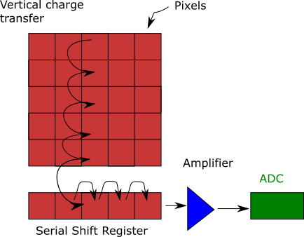
Figure 1. CCD carrier transport process
Complementary Metal Oxide Semiconductor (CMOS) technology
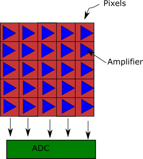
One of the biggest differences between CCD and CMOS sensors is that each pixel on the CMOS has its own amplifier. Not only that, but each column has its own ADC: once a pixel detects light, it will amplify it and then connect to the ADC for that column. In some configurations, each pixel may have its own ADC. A consequence of this configuration is that it is possible to read several pixels simultaneously (in a parallel configuration).
Some of the main advantages are that CMOS devices have lower power consumption than CCDs, the price of manufacturing is lower than CCDs, and they are faster in processing signals than CCDs. They are therefore ideal for fast image acquisition. Additionally, CMOS sensors can be fabricated using semiconductors besides silicon (like gallium arsenide, silicon germanium, indium gallium arsenide). These materials allow for CMOS to be sensitive to wavelengths beside the visible spectrum. All these are great advantages, especially if you are designing consumer electronic devices like digital cameras, or cell phones where battery life and cost are quite important.
Their biggest disadvantage is that all those extra amplifiers and ADCs create a lot of noise.

Figure 2. CMOS reading process. Electronics are integrated in each pixel
Resolution
It is important to pick the right camera that allows us to have the correct resolution for our application. For this discussion, we will assume that we are choosing a camera for a microscopy application.
Let’s calculate the minimum resolution for a 40x microscope objective with a Numerical Aperture of 0.65. We will use the Rayleigh criterion for this calculation: the minimum distance between two samples so that they can still be distinguished in the image plane. We can express this in the following equation:
![]()

where x is the distance between two samples, λ is the wavelength, NA is the numerical aperture, and n is the refractive index between the sample and the microscope objective. Assuming a wavelength of 550 nm (middle of the visible spectrum), an NA of 0.65 and n = 1 (air), we get a minimum separation of 540 nm. This separation is magnified 40x by the objective lens and will image on the sensor at a size of 21.6 μm. It may be easy to think that we will need at least a pixel size of 21.6 μm; we would like however for that image to cover at least 3 pixels. We will therefore need a pixel size of 7.2 μm or less.
In addition to this, we still need to consider camera noise and the quality of the optical elements. The resolution and performance of the camera can be characterized by the modulation transfer function (MTF), which is the ability of the camera and optical system to transfer a high contrast image at different resolutions.
Dynamic Range
Any kind of photodetector will have inherent noise. There is nothing we can do about it–that noise is the result of some quantum effects caused by temperature (dark noise) and caused by the electronics process during the AD conversation and amplification (read noise). If our capture photo signal is lower than the total noise of the system, we won’t be able to detect that signal and that will be our lower limit of detection. Our signal however cannot be infinitely large. Remember that once photo-electrons are generated, they are stored in a quantum well. That well has a finite capacity and if we exceed that capacity, we saturate the reading of that pixel. In effect, we have a minimum and a maximum range of photosignal that we can detect. That range is what we call a Dynamic Range. It can be measured in different ways depending on your applications. In photography, for example, it is measured in “stops,” whereas in microscopy, it is more common to measure it as a ratio (1000:1), in decibels (dB), or bit-depth. For example, 8-bit depth is approximately 50 dB. Regardless of the units, the concept is the same.
Let’s say you want to increase the Dynamic range of a sensor. You could increase the size of your quantum well, but that will also increase the size of your pixel, and if you increase the pixel’s size, you will reduce the device resolution. If you make the pixel too small to increase resolution, you will increase the dark noise, and, in the case of CMOS, you will need to find a space for all the electronics.
CMOS devices tend to have a higher dynamic range than CCD (although not always). One reason is that CCD tend to have very noisy electronics (that higher energy use has additional consequences), but high end CCD cameras can have a quantum efficiency of 90% (meaning that for every 100 photons received, 90 are converted to photo-electrons), while CMOS can have around 40%.
Fun Fact: The cones and rods in our eyes have a quantum efficiency of less that 2%
Confused, just wait…
Researching for this topic, I fell into a rabbit hole. There is so much information out there that it could be possible to teach a whole semester on the topic and only just scratch the surface. One thing to remember is that CMOS is a more recent technology than CCD and therefore there have been important advances in the last 10 years. Ten years ago, the choice between CCD and CMOS was less confusing: if you needed scientific, high precision images, you went with CCD. You sacrificed speed and it cost you. If you needed consumer electronics or high speed images, you needed CMOS at a cost in resolution.
Now, we have CMOS cameras with 6.5 μm pixel size, 95% quantum efficiency, and 96 dB dynamic range. Personally I would not be surprised if CMOS becomes the dominant imaging technology in the next 10 years.