FPGA-Based Control & Interface Electronics for a Tunable NIR Spectrometer
Optics for Hire
491 Massachusetts Ave., Suite 206b · Arlington, MA 02474
www.opticsforhire.com · (781) 583-7810
1. Executive Summary
Optics for Hire provided multi-phase electronics engineering services to a near-infrared spectroscopy instrument company over a five-year engagement. The work spanned FPGA firmware development and board bring-up support for an early spectrometer platform, a full custom PCB design for a scanning-mirror tunable device controller, and detailed interface board analysis and debug for a CCD-based spectrometer.
Across these phases, OFH delivered FPGA and NIOS firmware, custom SMD PCB designs with full BOM, USB 2.0 high-speed interface implementation, analog front-end design for PbS and InGaAs photodetectors, and systematic diagnosis and remediation of USB, CCD voltage, CCD clock timing, and analog signal integrity issues.
Custom SMD PCB
Altera Cyclone III FPGA, FTDI USB 2.0 high-speed interface, dual 16-bit ADC channels, and multi-detector support
in a <60 × 96 mm footprint under 500 mW.
Systematic CCD interface debug
USB disconnection, voltage out-of-spec, clock timing, and analog signal chain failures resolved through
oscilloscope-based diagnostics with specific passive component corrections identified for each channel.
Full software stack delivered
FPGA firmware, NIOS II embedded software, USB driver, and complete C#/.NET Windows host application with real-time
image display and histogram analysis.
Sustained engineering partnership
Five years and three instrument generations, providing electronics engineering capability the client did not
maintain in-house.
2. Background
The client develops tunable near-infrared spectrometers used in chemical analysis, process monitoring, and medical diagnostics. NIR spectrometers based on tunable Fabry-Perot filters, scanning mirrors, or liquid crystal tunable elements require sophisticated control electronics to synchronize the tuning element with the detector readout: coordinating timing signals, digitizing photodetector output at high speed, and transferring data to a host PC at rates that demand USB 2.0 high-speed operation.
OFH was engaged across multiple instrument generations to provide electronics engineering support the client did not maintain in-house. The engagement covered three distinct phases, each addressing a different instrument variant or technology generation.
3. Phase 1: FPGA Firmware and Board Bring-Up (2008)
3.1 Scope
The first engagement involved FPGA firmware support and board bring-up assistance for an existing spectrometer platform. The client's team encountered issues during production programming of the Altera EPCS4 serial configuration device, a non-volatile memory that stores both the FPGA configuration bitstream and the embedded NIOS II soft-processor firmware. Boards that had been operating correctly were failing after reprogramming.
3.2 Issues Resolved
- EPCS4 reprogramming procedure: Clarified that the JIC (JTAG Indirect Configuration) file format combines both the FPGA configuration and NIOS firmware into a single programming file. Reprogramming the EPCS4 requires the JIC file to restore both correctly.
- Board version compatibility: Identified that a connector pinout mirror change between the first and subsequent board revisions meant the JIC file compiled for board revision 1 was not compatible with the remaining four boards. A separate firmware build was required for the mirrored connector layout.
- Programming documentation: Documented the standard download procedure for FPGA and NIOS in a single programming step, suitable for production use.
4. Phase 2: Scanning Mirror Tunable Device Controller
4.1 Project Scope
The second engagement was a full custom electronics design: a new control and interface board to adapt the client's existing tunable Fabry-Perot spectrometer platform to a resonant scanning mirror tunable element. The scanning mirror approach required different timing and control electronics compared to the original tunable filter design. Mirror position must be tracked in real time from the driver phase signals, synchronized precisely with the detector integration window, and the digitized spectral data transferred to the host PC at up to 1,000 spectral points per 1.3 ms — a data rate requiring USB 2.0 high-speed operation.
4.2 System Architecture
The board was designed around an Altera Cyclone III FPGA (EP3C10) as the central control element, coordinating all timing signals, managing data flow between the ADC, detector interface, and USB subsystem, and implementing the communication protocol. Key architectural decisions:
- USB interface: Upgraded to USB 2.0 high speed (480 Mbit/s) via the FTDI FT245R USB FIFO bridge, enabling the free-run acquisition bandwidth of approximately 8 MB/s required for 1,000-point spectra at 5 kHz scan rate. RS-232 retained for command-only communication at auto-baud rate for snapshot mode instrument control.
- ADC selection: 16-bit, 1.33 MSPS Analog Devices AD7983 (primary high-speed channel) and 16-bit 250 kSPS AD7685 (auxiliary channels for thermistor and slow signals). ADCs were placed on the board location offering the shortest signal path from the detector, prioritizing signal quality over cost.
- Detector interfaces: PbS detector (Hamamatsu P9217) and InGaAs PIN photodiode (Hamamatsu G5853) both supported, with switchable front-end gain stages using Analog Devices AD8615 rail-to-rail op-amps. Precision voltage references (ADR391/ADR392) maintain ADC accuracy across temperature.
- Resonant scanner interface: SC-3-5 scanner phase signals intercepted and digitally decoded in the FPGA to extract mirror position. All timing signals for scan synchronization generated by the FPGA.
- APD bias supply: Maxim MAX15031 80V boost converter provides adjustable APD bias voltage for avalanche photodiode detector variants.
- Power management: LT3471 dual boost/inverter for analog rails, LM3671 step-down converters for FPGA and digital 3.3V and 1.2V rails, LP3874 LDO for precision analog 2.5V reference supply. Total power budget under 500 mW.
4.3 Electrical Specifications
| Parameter | Specification |
|---|---|
| Primary FPGA | Altera Cyclone III EP3C10, 144-pin EQFP, 50 MHz clock (Abracon ASE-50.000MHZ) |
| Configuration memory | Altera EPCS4, 4 Mbit serial flash (FPGA + NIOS firmware) |
| USB interface | FTDI FT245R USB/Parallel FIFO, USB 2.0 Full Speed (upgradeable to HS) |
| RS-232 interface | Maxim MAX3232E, auto baud rate, command protocol only |
| Primary ADC | Analog Devices AD7983, 16-bit, 1.33 MSPS PulSAR, MSOP/QFN |
| Auxiliary ADCs | Analog Devices AD7685, 16-bit, 250 kSPS (x2, for slow channels) |
| Voltage references | ADR391 (1.2V), ADR392 (2.5V), ADR130 (sub-bandgap), Analog Devices |
| Op-amps (signal chain) | AD8615 CMOS rail-to-rail, 20 MHz, precision (x4) |
| Op-amps (biasing) | LF353 JFET dual (x6, for detector bias networks) |
| Detector inputs | PbS (Hamamatsu P9217), InGaAs PIN (Hamamatsu G5853) |
| Resonant scanner | EOPC SC-3-5, 7×7 mm and 12×7 mm, up to 5 kHz |
| Data acquisition speed | Up to 1,000 points in 1.3 ms (1,000-point option) |
| Integration time range | 0.5 ms to 30 s, 0.5 ms steps |
4.4 Board Overview
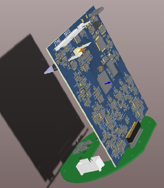
Figure 1: 3D rendered view of the custom spectrometer interface board. Altera Cyclone III FPGA (center), FTDI USB FIFO, ADC ICs, power management section, and CCD interface connector. JTAG programming header at upper left. Full analog, digital, and power management circuitry within the <60 × 96 mm form factor.
The completed board was delivered as a compact SMD assembly targeting the <60 × 96 mm form factor. The design includes JTAG programming access for FPGA firmware updates, power connectors, USB and RS-232 interface ports, and the CCD connector for the detector daughter board.
4.5 Deliverables
- 5 pieces of debugged, functioning prototype boards
- Complete BOM with US distributor part numbers (Digi-Key, Mouser, Newark)
- Schematics and PCB layout in Altium Designer (native format)
- FPGA firmware source code (Quartus project, VHDL/Verilog)
- NIOS II embedded software source code and compiled binary (.hex)
- USB driver source code for FTDI FT245R
- Sample host PC program in C/C++
- Hardware and software user documentation
- Detailed system design description for system integrator handoff
5. Phase 3: CCD Interface Board Analysis and Debug (2013)
5.1 Scope
In 2013, OFH was re-engaged to perform a systematic hardware and firmware analysis of the client's CCD-based spectrometer interface board. The board used a Perkin Elmer RL-series linear CCD array (RL1024PAG-021, RL1024PAQ-021, or RL2048PAQ-021) with an FTDI FT2232 dual-channel USB interface. The client was experiencing intermittent USB disconnections and unreliable CCD readout. OFH performed a structured diagnostic program covering the USB interface, CCD voltage levels, CCD clock timing, and the analog signal chain.
5.2 USB Interface Diagnosis
OFH developed a custom USB test program to isolate the FT2232 connectivity issues, enabling systematic characterization of USB device behavior under different cable and hub conditions. The diagnostic identified two root causes:
- Insufficient USB bus current: The USB port could not provide the current required by the FT2232 in high-speed mode. Oscilloscope measurement showed signal amplitude reduction on the FTDI clock output when using the failing cable. Resolution: specify use of a dual-power USB cable (drawing power from two USB ports) with an integrated ferrite filter.
- USB hub noise sensitivity: Certain USB 2.0 hubs inject sufficient noise onto the USB lines to cause the FT2232 to hang. Resolution: add 47 pF capacitors to ground on both USB D+ and D- lines (reworked onto existing boards); specify a USB 2.0 compliant cable; update host software to detect a non-responsive device and perform automatic reconnection via Windows API.
5.3 CCD Socket Mechanical Problem
Physical inspection revealed that the CCD sensor socket had bent pins on the right side, preventing reliable seating of the sensor. The right side of the sensor could be inadvertently removed when the socket latch was closed. This was identified and documented before electrical measurements began, as a misseated sensor would have prevented any meaningful signal characterization.
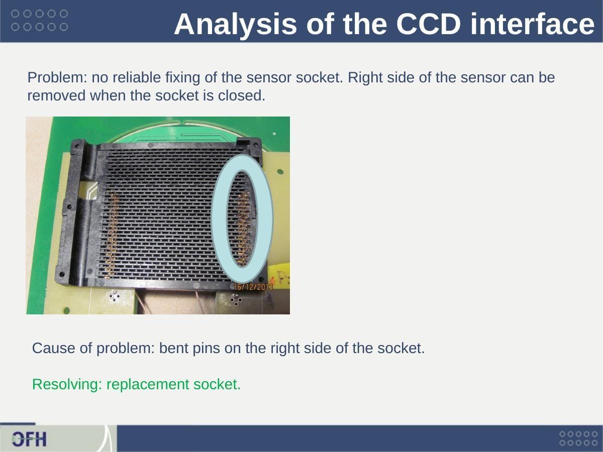
Figure 2: CCD sensor socket with bent pins on the right side preventing reliable retention of the sensor. Physical inspection identified this mechanical issue before electrical measurements began. Resolution: socket replacement.
5.4 CCD Voltage Level Analysis
OFH measured all CCD drive signal voltages with an oscilloscope and compared them against the Perkin Elmer CCD datasheet specifications. Multiple voltage levels were found out of specification across the vertical clock, supply, and horizontal clock domains.
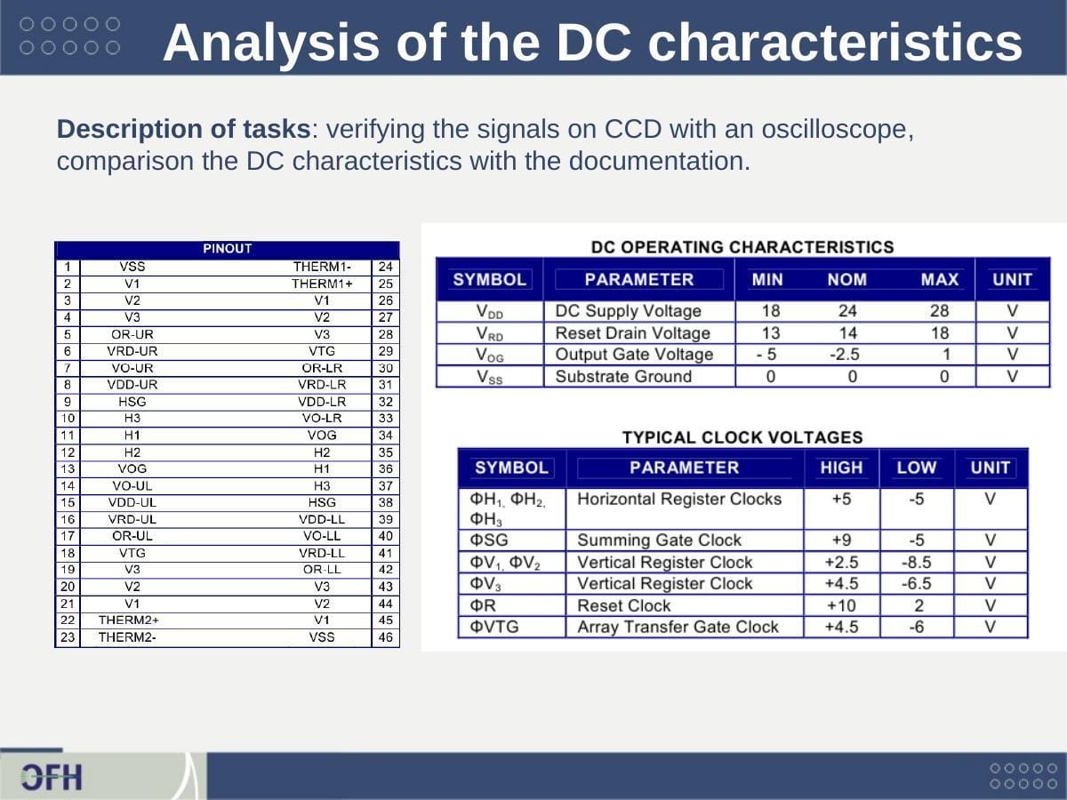
Figure 3: CCD pinout (46-pin) and DC operating characteristics from the Perkin Elmer RL-series datasheet, used as the measurement reference for all voltage analysis.
| Signal | Measured | Required | Resolution |
|---|---|---|---|
| V1, V2 vertical clocks (pins 2, 3 / 20, 21) | +5V (high) | +2.5V | Passive component correction in level-shifting circuit |
| V3 vertical clock low level | -9V | -6.5V | Passive component correction |
| VDD-UR supply (pin 8) | +12V | +24V | Passive component correction in charge-pump circuit |
| OR-UR (pin 5) | +10.5V | +10V (marginal) | Within margin; monitored |
| H1, H3 horizontal clocks (low level) | -6V | -5V | Passive component correction |
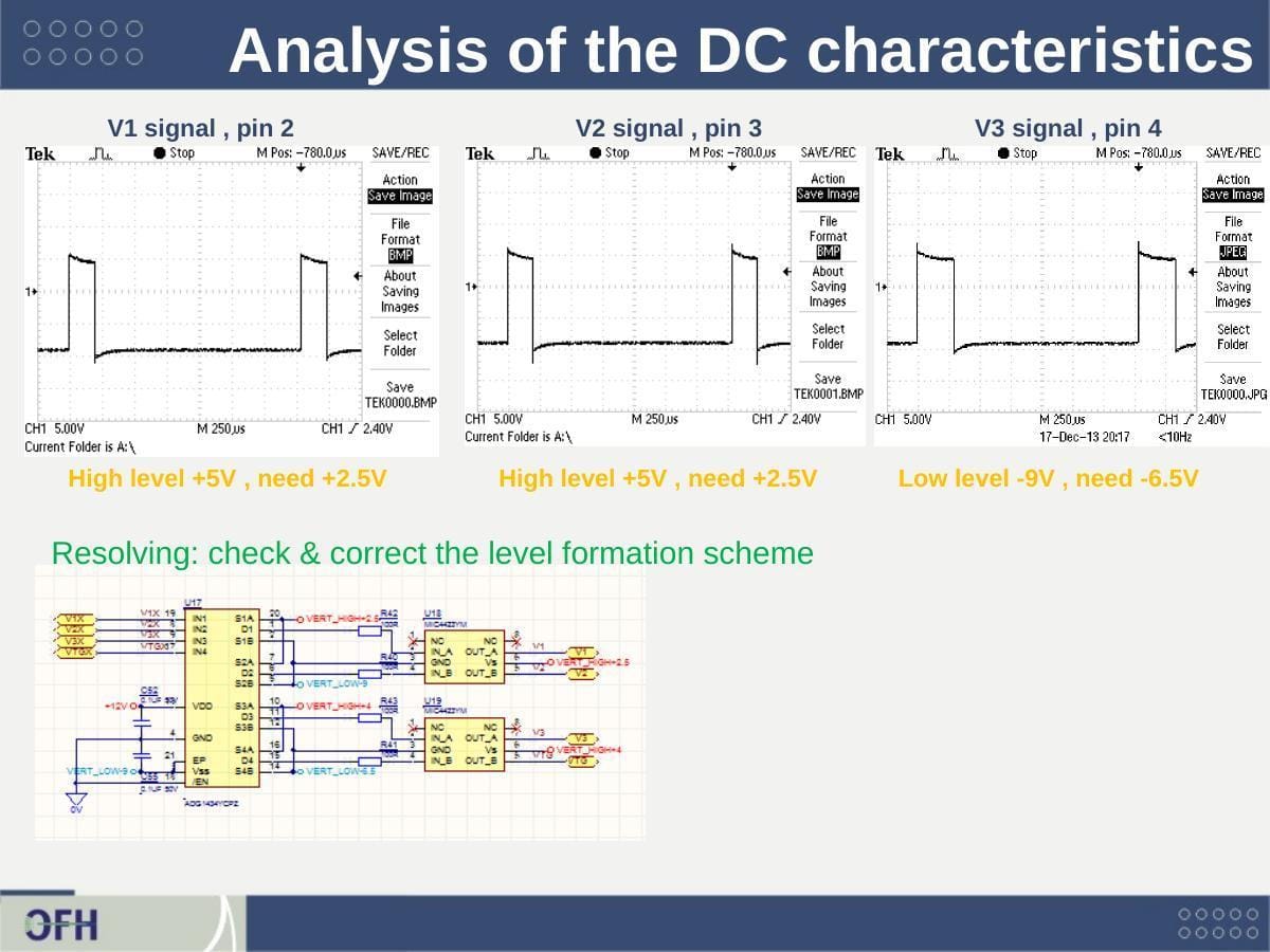
Figure 4: Oscilloscope measurements of V1 (pin 2), V2 (pin 3), and V3 (pin 4) vertical clock signals. V1 and V2 measured +5V high (required +2.5V); V3 measured -9V low (required -6.5V). Level formation schematic identifies passive components requiring correction.
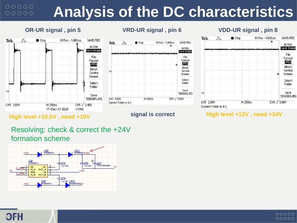
Figure 5: Oscilloscope measurements of OR-UR (pin 5), VRD-UR (pin 6), and VDD-UR (pin 8). VDD-UR measured +12V (required +24V). OR-UR measured +10.5V vs. required +10V (marginal). Charge-pump schematic identifies passive component corrections required.
All out-of-spec levels were traced to incorrect passive component values in the level-shifting circuits. Specific resistor and capacitor value corrections were identified for each affected channel, enabling targeted rework rather than board redesign.
5.5 CCD Clock Timing Analysis
Oscilloscope measurement of the CCD clock timing waveforms was performed and compared against the Perkin Elmer datasheet timing diagrams. One timing parameter was found out of specification:
- Vertical clock overlap time (V-ovl): Measured at 0 µs. Datasheet typical value: 26 µs. The V-ovl parameter is the period during which vertical clock signals V1 and V2 are both high during a vertical shift. A value of 0 µs indicates V2 transitions high before V1 goes low, eliminating the required overlap. Resolution: FPGA firmware timing parameter correction.
All other timing parameters including horizontal clock frequency (400 kHz) and reset clock pulse width (300 ns) were within specification.
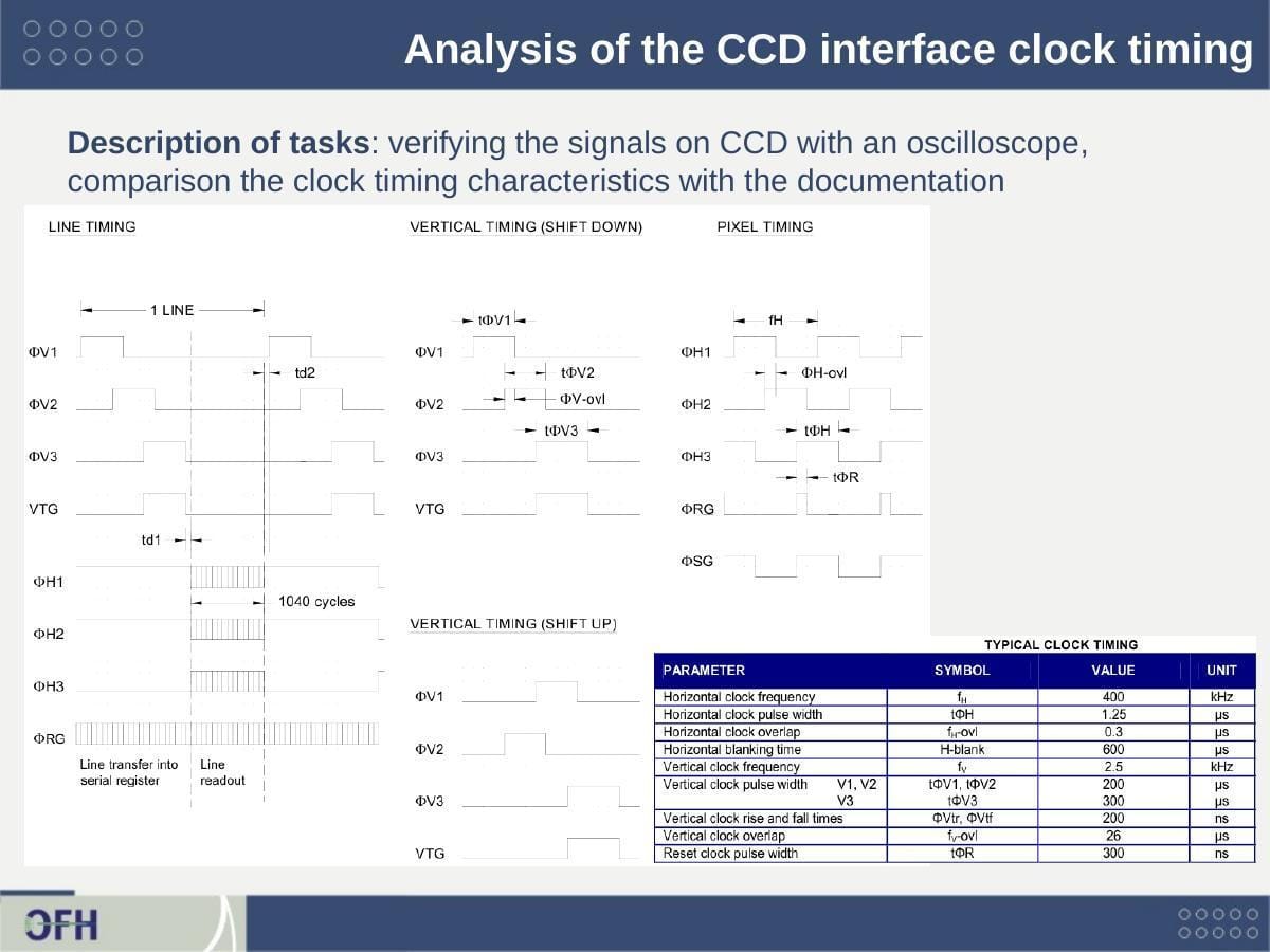
Figure 6: CCD interface clock timing diagram from the Perkin Elmer datasheet, covering line timing, vertical timing (shift down and shift up), and pixel timing. Key specifications: horizontal clock frequency 400 kHz, vertical clock overlap fv-ovl = 26 µs, reset clock pulse width tR = 300 ns.
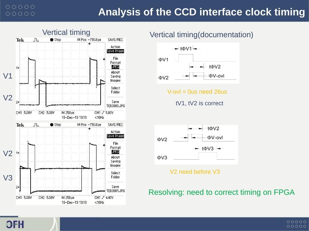
Figure 7: Oscilloscope measurement of CCD vertical clock timing showing the V-ovl defect. Measured V1/V2 waveforms show V2 transitioning high before V1 goes low, giving V-ovl = 0 µs. Datasheet requires 26 µs overlap. Resolution: FPGA firmware timing parameter correction.
5.6 Analog Front-End and Black Level Calibration
Analysis of the pre-amplifier circuit with no input signal (black level measurement) revealed a systematic offset difference between the two CCD output channels. This offset would manifest as a brightness difference between the two halves of the image when the channels are interleaved. Resolution: the FPGA firmware was updated to measure and store the individual black-level offset for each channel at startup and subtract it digitally during image reconstruction, eliminating the brightness artifact without requiring analog component changes.
5.7 Host Application Software
OFH delivered a complete Windows host application (C#/.NET Framework 4) providing a graphical interface for the spectrometer system. Key features:
- Dual communication interfaces: USB (automatic initialization and device detection with error diagnostics) and RS-232 (selectable COM port, auto baud rate detection with status confirmation)
- CCD acquisition control: Pixel readout frequency selection, integration time in milliseconds, frames addition with optional averaging (1 to 32 frames), operation mode (cyclic or single capture), and external trigger synchronization
- Binning control: Variable binning from 1x (full 2048 × 2048) to 1024x (2048 × 2 pixels), supporting both full-resolution and signal-averaging configurations
- Temperature monitoring: Onboard ADC temperature, dual CCD thermistor readout, and TEC PWM duty cycle control with resolution below 0.0001
- Image display and analysis: Real-time image viewer with contrast stretch, fit-to-window scaling, pixel coordinate and 16-bit intensity readout, and histogram analysis of user-selected regions with standard deviation and average statistics
6. Technical Significance
This multi-phase engagement demonstrates OFH's capability to provide sustained electronics engineering support across the full lifecycle of a photonics instrument, from new board design through production bring-up and field debug. Key technical contributions across the three phases:
- Complete software stack delivered: Full C#/.NET Windows GUI enabling CCD acquisition control, TEC management, USB and RS-232 communication, real-time image display with histogram analysis, and 16-bit data export. Delivered alongside the hardware and firmware as a turnkey instrument operation environment.
- FPGA and NIOS system architecture for a high-speed spectrometer controller: Coordinating resonant scanner phase decoding, multichannel ADC acquisition at 1,000 points per 1.3 ms, and USB 2.0 high-speed data transfer to the host PC.
- Custom SMD PCB with complete US-sourced BOM: Altera Cyclone III FPGA, FTDI USB FIFO, 16-bit ADCs, precision voltage references, and multi-rail power management in a compact (<60 × 96 mm) board under 500 mW.
- Mixed-signal board design discipline: Separate analog and digital ground planes joined at a single point, precision reference supply routing, and ADC placement for optimal signal quality, all confirmed as important corrective factors during the Phase 3 analysis.
- Systematic USB interface debug methodology: Test program development, oscilloscope-based signal characterization, and root-cause identification of both hardware (bus current, line noise) and software (reconnection logic) failure modes.
- CCD interface analysis: Quantitative comparison of all drive voltage levels and timing parameters against datasheet specifications, with specific passive component corrections identified for each out-of-spec signal, enabling targeted rework rather than board redesign.
From custom FPGA firmware and PCB design through systematic oscilloscope-based hardware debug and a complete C#/.NET host application, OFH delivered a full electronics engineering stack across three instrument generations and five years, providing capabilities the client did not maintain in-house.
7. About Optics for Hire
Optics for Hire (OFH) is an optical engineering consultancy based in Arlington, Massachusetts, with R&D teams in the United States and Europe. Since 2002, OFH has delivered optical engineering services across more than 800 unique programs, from startup prototypes to Fortune 50 production systems.
OFH capabilities relevant to this work include FPGA design (Altera/Intel, Xilinx) including embedded soft-processor development, custom SMD PCB design in Altium Designer, high-speed ADC and DAC interface design for photodetector and CCD readout, USB 2.0 interface implementation, CCD and photodetector front-end electronics, power management for precision analog/digital mixed-signal boards, and board bring-up and systematic signal integrity analysis.
Notable related programs include:
- First commercial LiDAR lenses for autonomous vehicles — Velodyne / Google Waymo, 2006
- Depth-sensing imaging optics — PrimeSense (acquired by Apple), 2009
- DNA sequencer optics — Illumina, 2010
- Closed-loop autofocus servo systems for semiconductor wafer processing — Carl Zeiss SMS, 2024–2025
| Illumination Design | Imaging Lens Design | Electronics & Software | System Prototyping |
|---|---|---|---|
| LED & laser illumination, medical, DOE optics | Self-driving car optics, ophthalmoscopes, endoscopes, night-vision | FPGA, PCB design, USB interfaces, CCD readout, closed-loop motion control | Laser spectrometers, optical metrology, 3D sensing |
Relevant Expertise
- FPGA design (Altera/Intel Cyclone, Xilinx) and NIOS II embedded software
- Custom SMD PCB design in Altium Designer: analog, digital, and mixed-signal
- CCD and photodetector front-end electronics (PbS, InGaAs, silicon PIN, APD)
- USB 2.0 high-speed interface implementation
- Systematic hardware debug: oscilloscope-based signal integrity analysis
- Complete BOM generation with US distributor sourcing